Product Summary
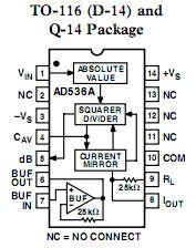
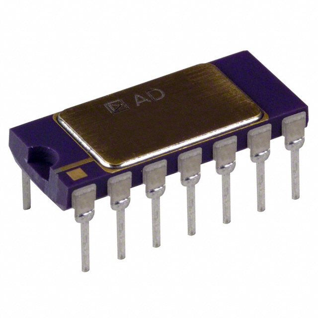
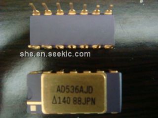
The AD536AJD is a complete monolithic integrated circuit which performs true rms-to-dc conversion. It offers performance which is comparable or superior to that of hybrid or modular units costing much more. The AD536AJD directly computes the true rms value of any complex input waveform containing ac and dc components. It has a crest factor compensation scheme which allows measurements with 1% error at crest factors up to 7. The wide bandwidth of the AD536AJD extends the measurement capability to 300 kHz with 3 dB error for signal levels above 100 mV. The AD536AJD is laser trimmed at the wafer level for input and output offset, positive and negative waveform symmetry (dc reversal error), and full-scale accuracy at 7 V rms. As a result, no external trims are required to achieve the rated unit accuracy.
Parametrics
AD536AJD absolute maximum ratings: (1)Supply Voltage: Dual Supply:±18 V, Single Supply:+36V; (2)Internal Power Dissipation:500mW; (3)Maximum Input Voltage:±25V Peak; (4)Buffer Maximum Input Voltage:±VS; (5)Maximum Input Voltage:±25V Peak; (6)Storage Temperature Range:–55℃ to +150℃; (7)Operating Temperature Range:0℃ to +70℃; (8)Lead Temperature Range(Soldering 60 sec):+300℃; (9)ESD Rating:1000V.
Features
AD536AJD features: (1)True RMS-to-DC Conversion; (2)Laser-Trimmed to High Accuracy: 0.5% Max Error; (3)Wide Response Capability: Computes RMS of AC and DC Signals, 450 kHz Bandwidth: V rms > 100 mV, 2 MHz Bandwidth: V rms > 1V, Signal Crest Factor of 7 for 1% Error; (4)dB Output with 60 dB Range; (5)Low Power: 1.2 mA Quiescent Current; (6)Single or Dual Supply Operation; (7)Monolithic Integrated Circuit.
Diagrams

| Image | Part No | Mfg | Description |  |
Pricing (USD) |
Quantity | ||||||||||||||||
|---|---|---|---|---|---|---|---|---|---|---|---|---|---|---|---|---|---|---|---|---|---|---|
 |
 AD536AJD |
 |
 IC TRUE RMS/DC CONV 14-CDIP |
 Data Sheet |

|
|
||||||||||||||||
 |
 AD536AJDZ |
 |
 IC TRUE RMS/DC CONV 14-CDIP |
 Data Sheet |

|
|
||||||||||||||||
 (China (Mainland))


